Silicon carbide (SiC) ib qho khoom siv lead ua muaj qhov sib txawv loj ntawm qhov dav (~Si 3 npaug), siab thermal conductivity (~Si 3.3 npaug lossis GaAs 10 npaug), siab electron saturation migration rate (~Si 2.5 zaug), siab tawg hluav taws xob teb (~ Si 10 zaug lossis GaAs 5 zaug) thiab lwm yam zoo heev.
Cov khoom siv semiconductor thib peb feem ntau suav nrog SiC, GaN, pob zeb diamond, thiab lwm yam, vim tias nws qhov sib txawv ntawm qhov dav (piv txwv li) ntau dua lossis sib npaug rau 2.3 electron volts (eV), tseem hu ua wide band gap semiconductor cov ntaub ntawv. Piv nrog rau thawj thiab thib ob tiam semiconductor cov ntaub ntawv, lub thib peb tiam semiconductor cov ntaub ntawv muaj qhov zoo ntawm high thermal conductivity, siab tawg hluav taws xob teb, siab saturated electron migration tus nqi thiab siab bonding zog, uas yuav ua tau raws li cov kev cai tshiab ntawm niaj hnub electronics technology rau siab. kub, siab zog, siab siab, siab zaus thiab hluav taws xob tsis kam thiab lwm yam mob hnyav. Nws muaj qhov tseem ceeb ntawm daim ntawv thov kev cia siab nyob rau hauv kev tiv thaiv lub teb chaws, aviation, aerospace, roj kev tshawb nrhiav, kho qhov muag, thiab lwm yam, thiab tuaj yeem txo qis zog los ntawm ntau tshaj 50% hauv ntau qhov kev lag luam xws li kev sib txuas lus broadband, hnub ci zog, kev tsim tsheb, semiconductor teeb pom kev zoo, thiab daim phiaj ntse, thiab tuaj yeem txo cov khoom ntim ntau dua 75%, uas yog qhov tseem ceeb tshaj plaws rau kev loj hlob ntawm tib neeg kev tshawb fawb thiab tshuab.
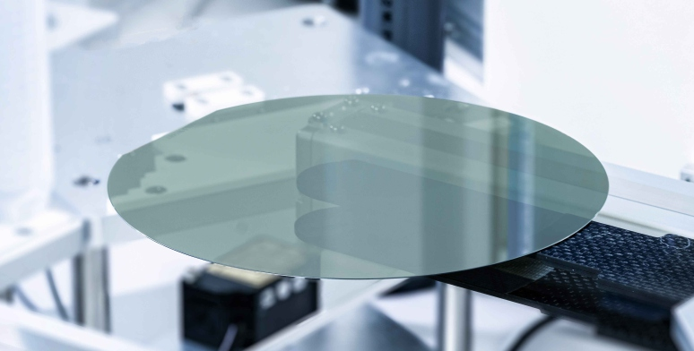
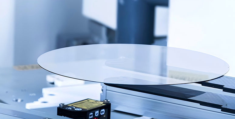
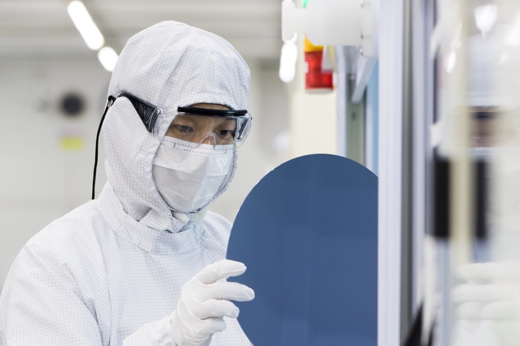
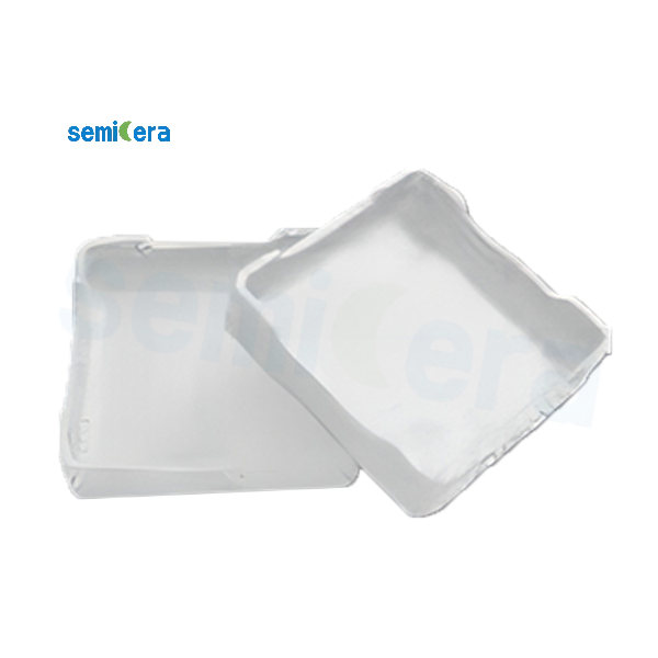
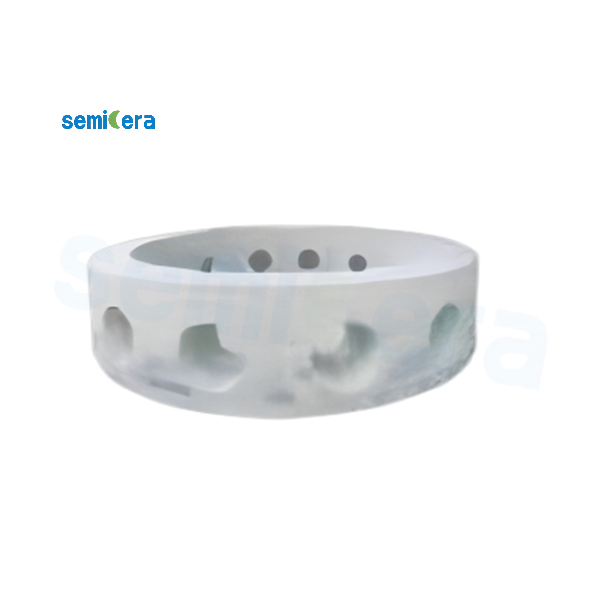
Semicera zog tuaj yeem muab cov neeg siv khoom zoo tshaj plaws Conductive (Conductive), Semi-insulating (Semi-insulating), HPSI (High Purity semi-insulating) silicon carbide substrate; Tsis tas li ntawd, peb tuaj yeem muab cov neeg siv khoom nrog homogeneous thiab heterogeneous silicon carbide epitaxial nplooj ntawv; Peb kuj tuaj yeem kho cov ntawv epitaxial raws li cov kev xav tau tshwj xeeb ntawm cov neeg siv khoom, thiab tsis muaj qhov tsawg kawg nkaus kom muaj nuj nqis.
WAFFERING SPECIFICATIONS
*n-Pm=n-type Pm-Grade,n-Ps=n-type Ps-Qib,Sl=Semi-lnsulating
| Yam khoom | 8-Inch | 6-Inch | 4-Inch | ||
| np | n- Pm | n-Ps | SI | SI | |
| TVV (GBIR) | ≤ 6 hli | ≤ 6 hli | |||
| Hneev (GF3YFCD) - Tus Nqi Tsis Muaj | ≤15μm | ≤15μm | ≤ 25μm | ≤15μm | |
| Warp (GF3YFER) | ≤ 25μm | ≤ 25μm | ≤ 40μm | ≤ 25μm | |
| LTV (SBIR)-10mmx10mm | < 2 m os | ||||
| Wafer Ntug | Beveling | ||||
NTAU NTAU
*n-Pm=n-type Pm-Grade,n-Ps=n-type Ps-Qib,Sl=Semi-Insulating
| Yam khoom | 8-Inch | 6-Inch | 4-Inch | ||
| np | n- Pm | n-Ps | SI | SI | |
| Nto tiav | Ob chav sab Optical Polish, Si- ntsej muag CMP | ||||
| SurfaceRoughness | (10um x 10um) Si-FaceRa≤0.2nm C-Face Ra≤ 0.5nm | (5umx5um) Si-Face Ra≤0.2nm C-Face Ra≤0.5nm | |||
| Ntug Chips | Tsis Muaj Kev Tso Cai (ntev thiab dav ≥0.5mm) | ||||
| Indents | Tsis Muaj Tso Cai | ||||
| Scratches (Si-Face) | Qty.≤ 5, Ua kom tiav Length≤0.5 × wafer txoj kab uas hla | Qty.≤ 5, Ua kom tiav Length≤0.5 × wafer txoj kab uas hla | Qty.≤ 5, Ua kom tiav Length≤0.5 × wafer txoj kab uas hla | ||
| Kev tawg | Tsis Muaj Tso Cai | ||||
| Ntug Exclusion | 3mm ib | ||||